We are excited to begin featuring the newest addition to our laboratory, the Bruker X4 Poseidon desktop micro-CT. This instrument represents the next step in high-performance desktop micro-CT imaging, offering a flexible platform that can be configured to meet the needs of a wide range of research laboratories. Going forward, the Bruker X4 Poseidon replaces both the SkyScan 1272 and SkyScan 1275 instruments in our portfolio.
Our X4 Poseidon combines a high-resolution transmission X-ray source, capable of an emission spot size down to 2 µm, with both a high-resolution sCMOS detector and a high-speed flat panel detector in Bruker’s MultiVision configuration. This dual-detector design provides researchers with the flexibility to balance resolution, field of view, and scan speed depending on the sample and imaging objective.
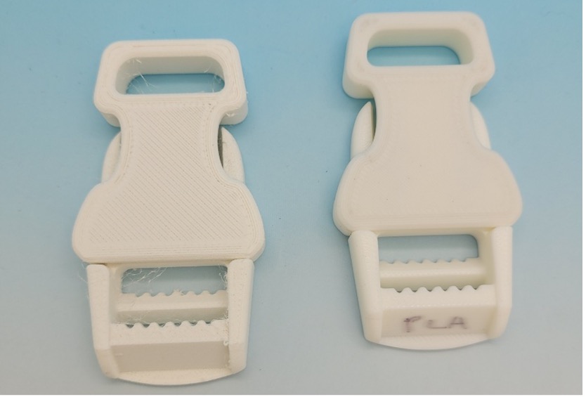
To demonstrate the system’s capabilities, we used the X4 Poseidon to examine an increasingly relevant application: 3D-printed materials. As fused deposition modeling (FDM) printers have become widely used, advances in filament materials are creating new opportunities to optimize printed parts for weight, density, strength, and performance. In this study, we compared a standard polylactic acid (PLA) filament with a specialized aerated “Air PLA” filament designed to reduce part weight and density while preserving functional performance. Using micro-CT, we were able to visualize and compare the internal structure of the printed materials, providing insight into how material formulation affects the final printed part.
X-Ray Microscopic Imaging – X4 Poseidon – MultiVision Configuration
To complete this quantitative assessment of differences between the two PLA filaments, we employed both the high-resolution sCMOS detector to image the ~1.75mm thick filaments as manufactured and the high-speed flat-panel detector to image snap buckles printed from each filament. In using the sCMOS detector, we obtain a detailed view within the thin filaments with an isotropic voxel size of 4 µm, which allows us to best visualize any pores 8-12 µm and above in diameter. Meanwhile, the flat-panel detector quickly examined the much larger, printed buckles at an isotropic voxel size of 20 µm to examine the parts for differences in macro-porosity. No other desktop instrument in our portfolio matches the capabilities of the X4 Poseidon in allowing us to quickly swap detectors without even requiring the sample to be removed or the instrument to be powered down.
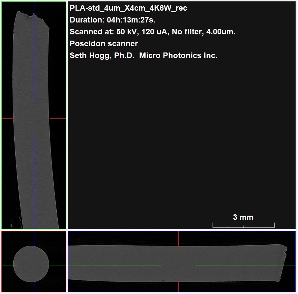
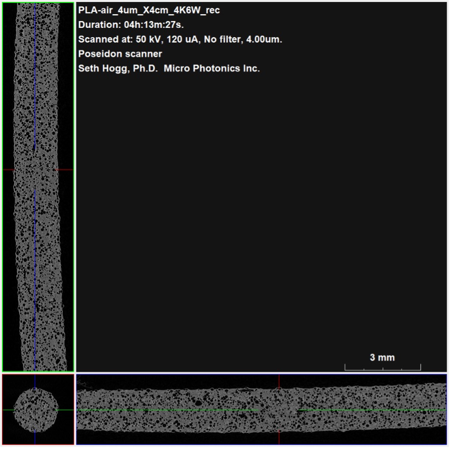
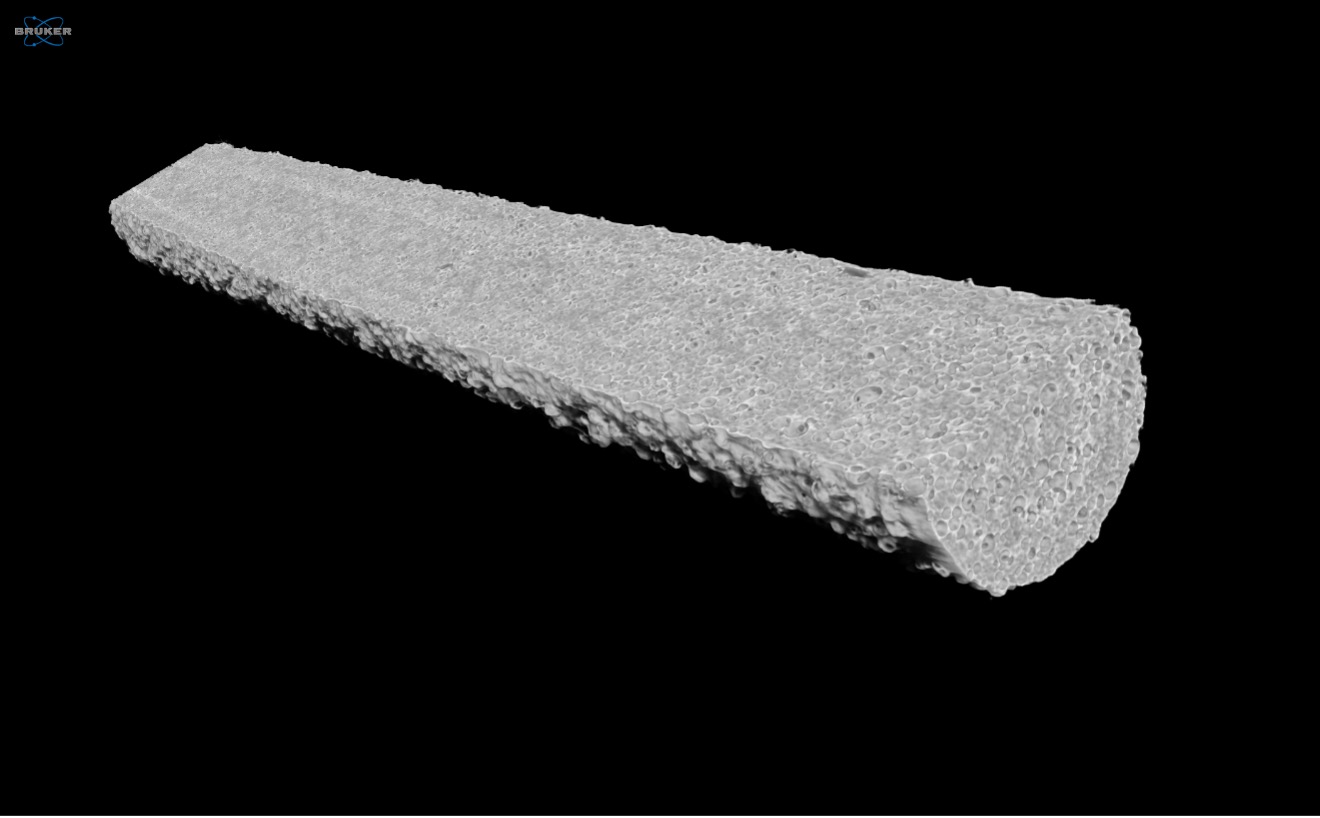
As shown in Figure 2, we used the high-resolution sCMOS detector to visualize differences in the as-manufactured features within each filament. The foamed porosity is quickly visible within the Air PLA sample whereas few pores are visible in the standard PLA filament. This observation supports the manufacturer’s claims regarding the special preparation of the functional Air PLA filament.
For this project, we utilized Bruker CTVox to render the volumetric data into an interactive dataset to further explore pore structures.Figure 3 provides a clipped view from within CTVox comparing the standard PLA and the Air PLA samples, further supporting our observations from DataViewer.
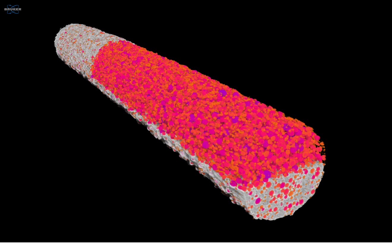
CTVox also allows us to overlay the quantitative pore data obtained from CTAn to visualize and map the location of pores in 3D space based on their calculated diameter. Figure 4 highlights a clipped view along a portion of the Air PLA sample with the quantitative pore data overlaid and colored based on calculated diameter. For the portion of the Air PLA filament examined, we used Bruker CTAnalyzer to calculate a global porosity of about 30% and an average pore diameter of 74.30 ± 26.38 µm. In contrast, the standard PLA was found to have a porosity of <1% and an average pore diameter of 14.71 ± 19.23 µm.
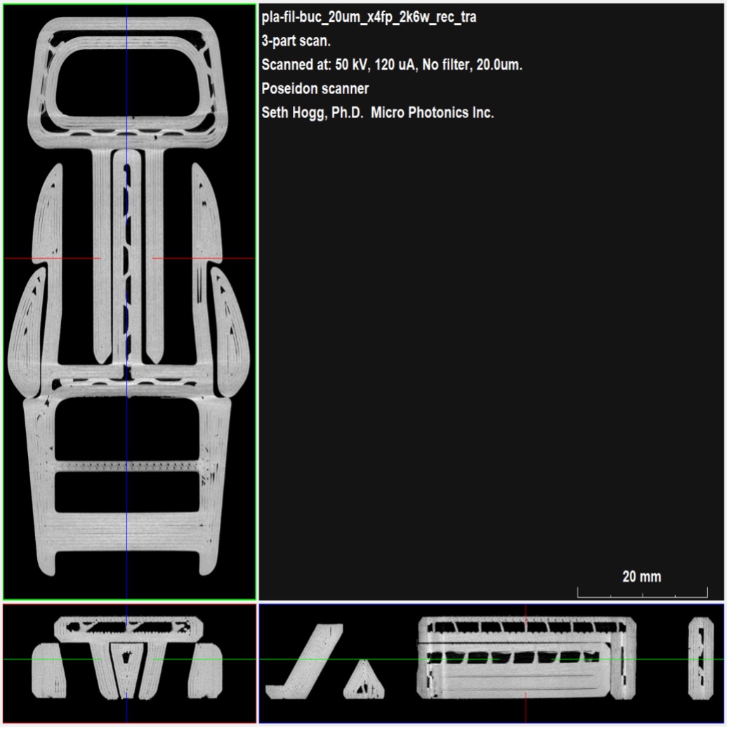
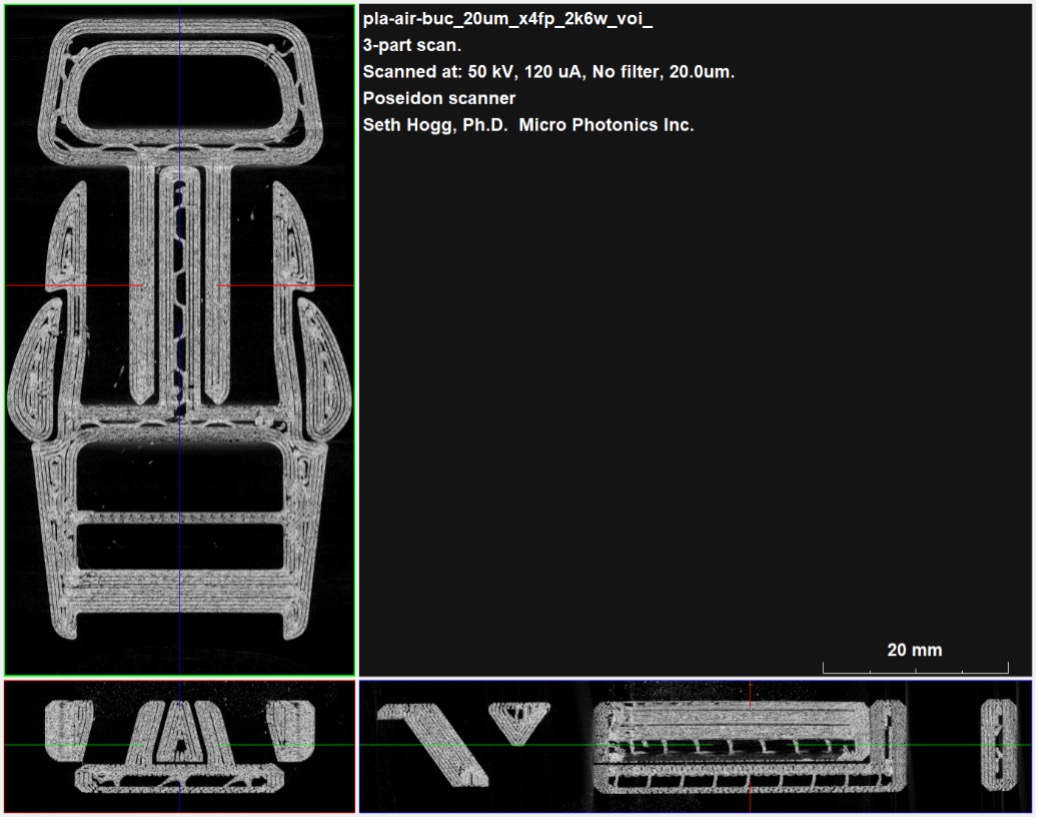
Figure 5 provides planar views through the 3D printed snap buckle models produced using the same file and the same printer but with the two different filaments. This test was designed to examine differences in how the final structures of printed parts differ based on the choice of FDM filament.
In examining the standard PLA print, large pore structures are visible as designed by the 3D slicer to keep part weights low and fill large solid regions of the model with sparse infill geometries. However, the clip produced with the Air PLA shows similar large pore structures but also shows a much higher incidence of very small pores throughout the structure. This qualitative view suggests that the highly porous Air PLA filament transfers some of the as-manufactured porosity into the final printed product despite going through a melting and re-solidification process during the deposition of the material within the 3D printer.
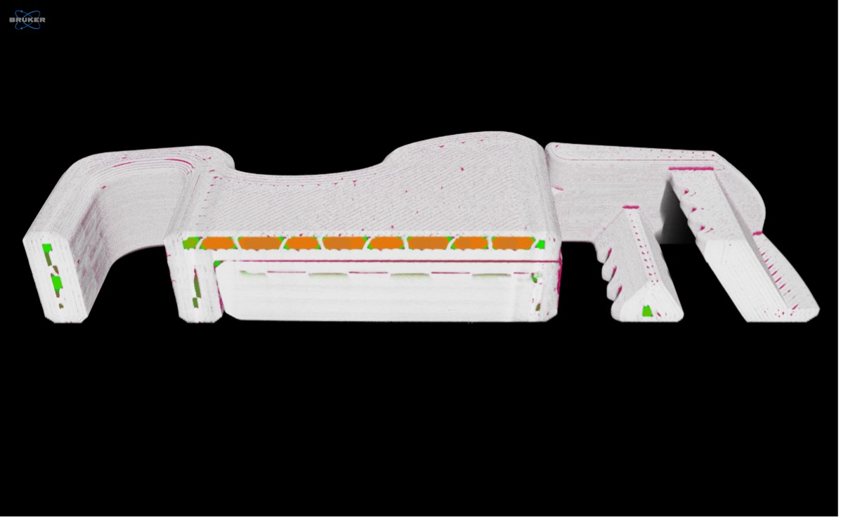
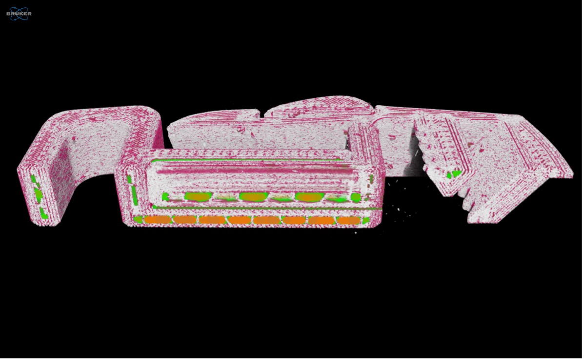
Figure 6 also provides a clipped view with CTVox combining both the reconstructed structural data along with the overlaid pore size distribution. As we noted qualitatively, both buckle samples have similar macro-porosity while the Air PLA sample appears to have a much higher population of small pores throughout the printed structures.
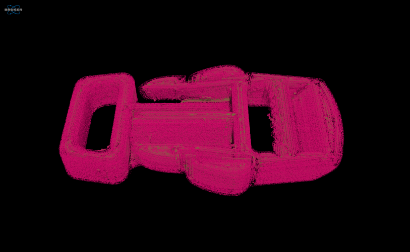
Figure 7 supports our view as shown in Figure 6 as well in directly comparing the location of the smallest pores within each sample dataset. While some small pores do exist in the sample printed from standard PLA, the isolated pore view from the Air PLA sample provides a striking visual difference in the volume of these small pores.
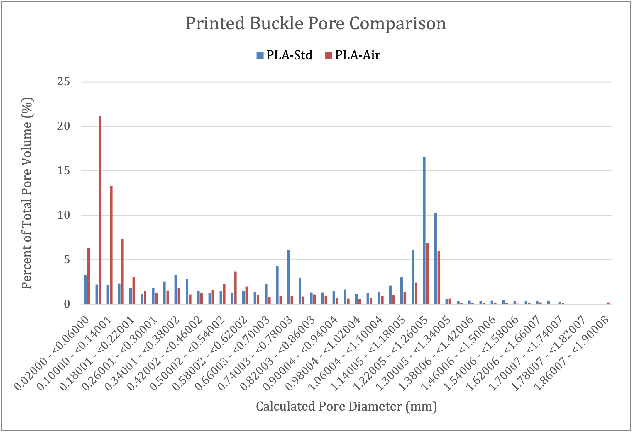
Moving a step beyond just visual comparison, Figure 8 highlights the quantitative difference in the total number of pores less than 300 µm in diameter as seen by the large spike in the histogram on the left side of the chart. Conversely, the standard PLA buckle sample shows the highest contribution to total pore volume arising from voids larger than 1 mm in diameter. As a reminder, these larger pores are the as-designed open volumes within the part as directed by the 3D Slicer in preparing the model for printing. While both buckle samples calculated to be about 12,400 mm3 in volume, the standard PLA buckle had a porosity of about 11% while the Air PLA buckle had a porosity of 25%.
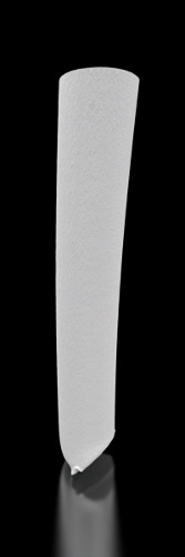
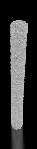
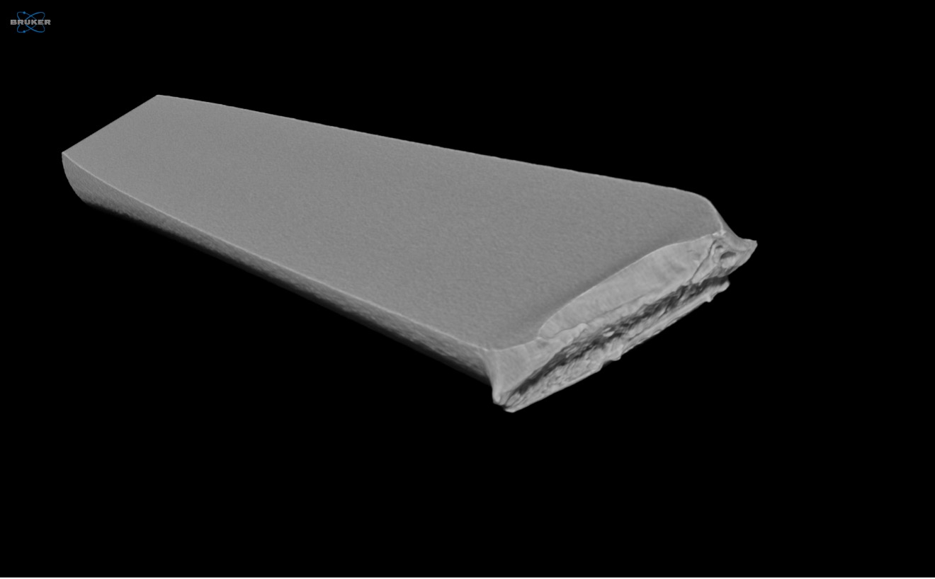
Figure 9: 3D rendering of the STL models created from the dataset of standard PLA (left) and Air PLA (right)
After analyzing the datasets using CTAn, we imported the filament datasets into Simpleware to create detailed volumetric meshes for each dataset. After the meshing process was completed, STL models for each filament dataset were output for rendering within Maverick Indie. Figure 9 highlights the notable differences between the two samples as the surface texture on the Air PLA sample is significantly more course arising from the high degree of porosity added to the filament during the manufacturing process. For this reason, the Air PLA filament will be considerably more abrasive during printing with FDM printers and should be coupled with a hardened steel nozzle rather than a brass nozzle to minimize the damage occurring to the nozzle during printing.
Conclusion
Micro-CT is a versatile technique that can image almost any sample type that both fits within the instrument and allows for X-ray energy to pass through without full attenuation. As our latest step forward in imaging innovation, the Bruker X4 Poseidon desktop micro-CT is available in a unique MultiVision configuration which offers the ability to select your X-ray detector based on the specific needs of your samples on a per-sample basis. When the highest resolutions are needed, the sCMOS detector leaps into action and when speed and imaging volume is more important than resolution, a high-speed flat-panel detector rises to the challenge.
We hope you find this Image of the Month article informative and encourage you to subscribe to our newsletter and social media channels in preparation for the continuation of our Image of the Month series next month.
Scan Specifications
| Sample | Filament | Printed Buckle |
| Detector | sCMOS | Flat-panel |
| Voltage (kV) | 50 | 50 |
| Current (µA) | 120 | 120 |
| Filter | None | None |
| Voxel Size (µm) | 4 | 20 |
| Rotation Step (deg) | 0.2 | 0.3 |
| Exposure Time (ms) | 1420 | 90 |
| Rotation Extent (deg.) | 360 | 360 |
| Scan Time (HH:MM:SS) | 04:13:27 | 00:37:57 |
These scans were completed on our Bruker X4 Poseidon instrument at the Micro Photonics Imaging Laboratory in Allentown, PA. Reconstructions were completed using NRecon 2.0 while visualization and volumetric inspection of the 2D and 3D results were completed using DataViewer and CTVox. Quantitative assessments of porosity and pore size distribution were determined using Bruker CTAnalyzer (1.25.0.0). The datasets were converted to STL volumetric models using Synopsys’ Simpleware software with the CAD add-on module (Synopsys, Inc., Mountain View, USA) before 3D rendering using Maverick Render Indie (Random Control, Madrid, Spain).
Would you like your work to be featured in our monthly newsletter? If so, please contact us by calling Seth Hogg at 610-366-7103 or emailing seth.hogg@microphotonics.com.