
Understanding the difference between spot size, voxel size, detector sampling, and spatial resolution
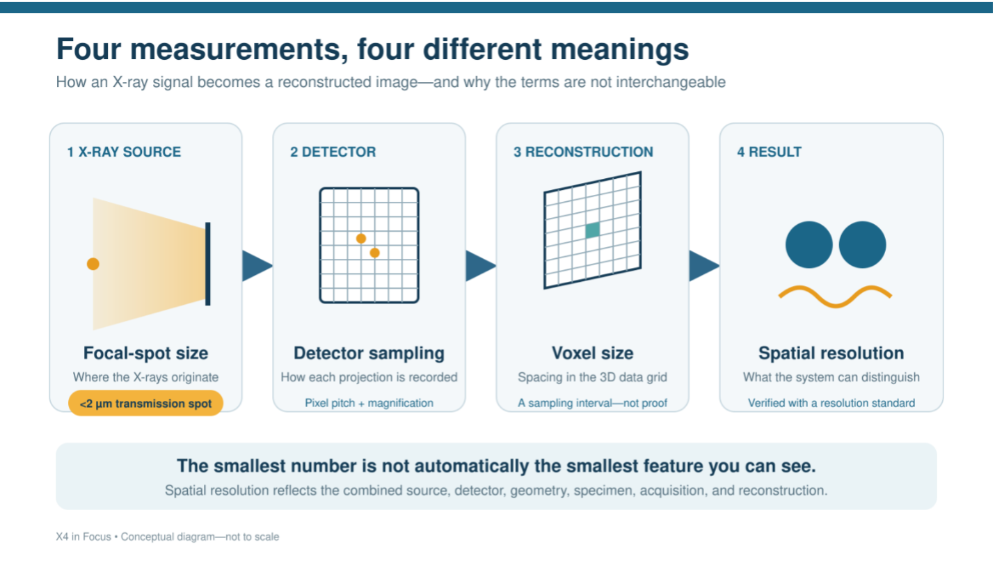
A specification of 2 µm can sound like a simple statement of image resolution. In micro-CT, however, focal-spot size, detector sampling, voxel size, and spatial resolution describe different parts of the imaging process. A 2 µm value for one cannot be assumed to mean 2 µm for the others.
For the X4 POSEIDON, 2 µm refers to both the focal-spot capability of the transmission X-ray source and the system’s demonstrated ability to resolve 2 µm features under appropriate high-resolution conditions. It does not mean that every scan has a 2 µm voxel size or that 2 µm structures will be visible in every specimen.
What does the X4’s 2 µm specification refer to?
Bruker specifies the X4 POSEIDON transmission source as producing an X-ray focal spot smaller than 2 µm at 2 W. The focal spot is the small area within the source from which the X-rays originate.
Bruker also documents the ability of an X4 configured with the transmission source and sCMOS detector to resolve 2 µm features in calibrated 2D and 3D resolution standards.
These are related but distinct statements. The small focal spot helps reduce image blur, while the demonstrated resolution reflects the performance of the complete imaging system under defined test conditions.
What is X-ray focal-spot size?
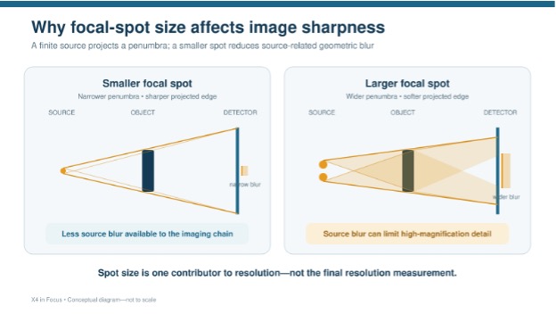
The focal spot is not an image pixel or a reconstructed voxel. It is a physical characteristic of the X-ray source.
Ideally, X-rays would originate from a single point. In practice, they are generated across a small area. As that area becomes larger, the edges of projected features can become less sharply defined, particularly at higher geometric magnification.
A smaller focal spot therefore supports higher-resolution imaging by limiting source-related blur. It creates the conditions needed to distinguish small features, but it does not determine the final image resolution by itself.
How is voxel size different?
A voxel is the three-dimensional equivalent of a pixel. It is the smallest unit in the reconstructed volume and represents the spacing at which the data are displayed and analyzed in three dimensions.
Voxel size is influenced by the detector sampling, geometric magnification, selected field of view, and reconstruction settings. Moving a small specimen closer to the X-ray source can increase its projected size on the detector and produce a smaller object-side voxel.
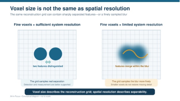
A small voxel creates a finer reconstruction grid. It does not guarantee that structures of the same size have been resolved. The scan may contain submicron voxels while its true spatial resolution remains limited by the focal spot, detector response, contrast, noise, movement, or other parts of the imaging chain.
What does detector sampling contribute?
The detector divides each X-ray projection into individual picture elements. The number and pitch of those detector elements affect how finely the projected image can be sampled.
The X4 flat-panel detector has a 2800 × 2400-pixel array, while the sCMOS detector has a 4096 × 4096-pixel array with finer detector sampling. Within the appropriate transmission-source and imaging-geometry architecture, the sCMOS detector can provide the additional sampling needed for high-resolution studies.
Detector pixel count alone does not establish spatial resolution. Its contribution depends on the physical detector characteristics, geometric magnification, field of view, source spot size, and the way the projection data are reconstructed.
What is spatial resolution?
Spatial resolution describes the system’s ability to distinguish two closely spaced structures as separate features. It is closer to what most researchers mean when they ask, “How small a feature can I actually see?”
Unlike voxel size, spatial resolution reflects the combined performance of the complete imaging system. It is influenced by:
- X-ray focal-spot size
- Detector sampling and detector response
- Source/sample/detector geometry
- Mechanical stability and sample movement
- Number and quality of the projections
- Signal-to-noise ratio and material contrast
- Reconstruction and image-processing settings
For this reason, spatial resolution is evaluated using calibrated test objects or methods such as line-pair patterns and modulation transfer measurements—not simply by reading the voxel dimensions from a reconstructed dataset.
Can a scan have voxels smaller than 2 µm?
Yes. The X4 can reconstruct submicron voxels when the specimen is small enough and the selected geometry provides sufficient magnification.
A submicron voxel size means that the reconstructed volume is being sampled on a submicron grid. It does not mean that the system has produced submicron spatial resolution or that every submicron structure can be distinguished.
A feature that occupies only one voxel may affect that voxel’s intensity, but it generally cannot be characterized or measured reliably from that information alone. Quantitative analysis usually requires the feature to be represented across multiple voxels with sufficient contrast.
How do sample size and scan geometry affect the result?
To increase geometric magnification, the specimen is positioned closer to the X-ray source and its projected image occupies more of the detector. This can improve object-side sampling, but it also reduces the field of view.
The specimen must remain fully within the usable imaging area as it rotates. Larger samples generally require less magnification and a broader field of view, resulting in larger voxels. Smaller samples—or small regions of interest—can often be positioned for higher magnification and finer sampling.
On the X4, the Advanced Stage and Best-Scan-Geometry architecture allow the relative positions of the source, specimen, and detector to be adapted to the sample. This helps the system use the available source and detector performance effectively rather than treating resolution as a fixed detector specification.
How does the X-ray source affect achievable resolution?
The X4 can be configured with either a reflection or transmission X-ray source. These sources support different imaging priorities.
The standard reflection source has a focal spot smaller than 5 µm at its specified operating condition. In that architecture, the source can become the limiting factor in high-magnification imaging, regardless of which detector is used.
The transmission source provides a focal spot smaller than 2 µm at its specified operating condition. When combined with the Advanced Stage, Best-Scan-Geometry, and appropriate detector, it reduces source-related blur and allows the system to take greater advantage of fine detector sampling.
This is why detector choice and source architecture should not be considered independently when evaluating resolution.
Why might a 2 µm feature still be difficult to see?
Feature visibility depends on more than feature size. A small structure with strong X-ray contrast may be easier to identify than a larger structure whose density is nearly identical to that of the surrounding material.
The ability to see or measure a feature can also be affected by:
- The material’s X-ray attenuation
- Feature orientation and shape
- Image noise
- Exposure and source power
- Sample movement
- Beam-hardening or metal artifacts
- Reconstruction and filtering choices
- The accuracy required for quantitative measurement
Resolving a high-contrast test pattern under controlled conditions is therefore different from detecting a subtle interface, fine crack, pore, fiber, or biological structure within a complex specimen.
Why not use the smallest possible voxel for every scan?
The smallest voxel is not automatically the best voxel.
Higher magnification reduces the field of view and may prevent the entire specimen from fitting within a single acquisition. Finer sampling can also increase scan time, reconstruction time, data volume, and sensitivity to movement without adding useful information if the structures of interest are comparatively large.
The practical objective is to use a voxel size and imaging geometry that adequately sample the smallest feature required by the research question. Additional sampling is valuable only when the rest of the system—and the specimen itself—can support the added detail.
How should a researcher plan a high-resolution scan?
The scan should begin with the feature that must be detected or measured, not with the smallest number available in the instrument specifications.
Important questions include:
- What are the overall dimensions of the specimen?
- What is the smallest feature that must be distinguished?
- How much contrast exists between that feature and its surroundings?
- Must the feature only be detected, or measured quantitatively?
- How much of the specimen must remain within the field of view?
- What acquisition time and data volume are practical?
- Which source, detector, and imaging geometry best support those requirements?
A sample evaluation can help determine whether the desired feature is visible with adequate contrast and whether the selected voxel size provides sufficient sampling for the intended analysis.
Reading the 2 µm Specification Correctly
The X4 POSEIDON’s 2 µm capability is not the result of a single component or setting. The transmission source’s small focal spot limits source-related blur, the sCMOS detector provides fine sampling, and the stage and imaging geometry position the specimen so those capabilities can be used effectively.
Spot size describes the X-ray source. Voxel size describes the reconstruction grid. Detector sampling describes how projection information is recorded. Spatial resolution describes what the complete system can distinguish.
Understanding those differences allows researchers to move beyond the smallest number on a specification sheet and ask the more useful question: What imaging configuration will reveal the feature that matters in this particular specimen?