
Rendered Video of a Porous Ceramic Filter
Porous ceramics are used for functional and structural applications from filtration, absorption, and catalysts to lightweight structural components. As filtration devices, they are used to remove contaminants — similar to how water from aquifers seeps through layers of rock, water in a porous ceramic filter permeates natural media to rid itself of impurities. We used micro-CT to examine a porous ceramic to quantify pore size distribution and porosity throughout a ceramic tube.
X-Ray Microscopy Imaging of Ceramics
To examine pore size and distribution within ceramic materials, we utilized the high-resolution SkyScan 1272 desktop micro-CT. Ceramic imaging is a great application for micro-CT as ceramics are rigid, have pore distributions, and are of reasonable density. For this study, we utilized a 2×2 binning of the 16MP CCD detector present in the SkyScan 1272 to image the entire ceramic cylinder at an isotropic voxel size of 8.5µm. The power to bin the detector in SkyScan instruments allows the user to best balance time and resolution for imaging as higher binning produces faster scans, albeit at lower resolutions.
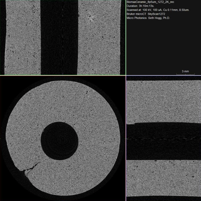
In inspecting the results from the ceramic cylinder, we see several distinct features present in DataViewer (Figure 2). From the image, we see the bulk ceramic, the pores distributed throughout, and defects such as the crack visible in the lower left image radiating from the outside of the cylinder towards the inside but not fully reaching the lumen.
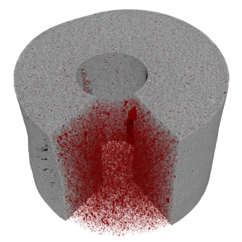
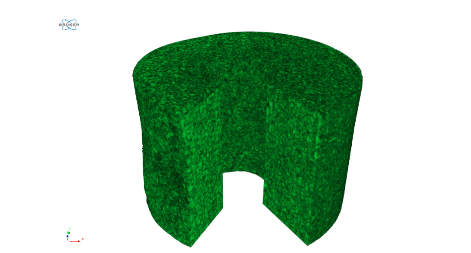
Moving to a volumetric rendering in CTVox, we see the presence of some extra ceramic deposits within the lumen as well as a large void inside one of the walls (Figure 3). The ability to interactively review imaging data in 3D from a SkyScan instrument within CTVox can often help identify unusual or interesting features of note within the sample that may not always be as evident from a planar 2D view.
After using CTAn to calculate the pore size distribution, a color-coded map of pores by diameter can be exported (Figure 4). For this sample, the average pore size was determined to be 42.1±25.7µm with an overall porosity of 4.9% of the volume of the cylinder.
Likewise, CTAn also allows us to quantify the thickness distribution of the ceramic to give us a better idea of the average thickness of the struts within the ceramic (Figure 5). For this cylinder, the average thickness was 183±45.0µm with a total volume of about 3000 mm3 and a surface area of about 20000mm2.
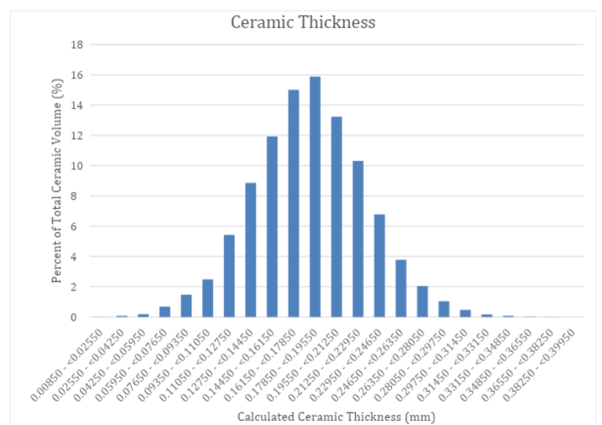
Examining the quantitative analysis results further, we extracted the size distribution plot from the ceramic portion of the sample (Figure 5). In this case, we see a normal Gaussian distribution centered around the average thickness of the sample (~180µm). If the sample had distinct regions of higher and lower porosity we would instead expect to see multiple peaks in the distribution. The single Gaussian peak present in this sample tells us that the pore distribution is fairly uniform throughout the sample despite the presence of a few larger pores identified earlier.
Conclusion
The SkyScan 1272 provided both the appropriate power and the resolution to image a ceramic filtration cylinder. Both the quantitative pore distribution as well as the thickness distribution of the ceramic were determined, allowing us to examine the uniformity of the pore distribution within the sample. We hope you found this Image of the Month informative and encourage you to subscribe to our newsletter and social media channels in preparation for the continuation of our image of the month series next month.
Scan Specifications
| Sample | Ceramic Cylinder |
| Voltage (kV) | 100 |
| Current (µA) | 100 |
| Pixel Size (µm) | 8.5 |
| Rotation Step | 0.2 |
| Scan Time (HH:MM:SS) | 03:10:13 |
These scans were completed on our desktop SkyScan 1272 system at the Micro Photonics Imaging Laboratory in Allentown, PA. Reconstructions were completed using NRecon 2.1 and visualization of 2D and 3D results were completed using DataViewer and CTVox.
Would you like your work to be featured in our monthly newsletter? If so, please contact us by calling Seth Hogg at 610-366-7103 or e-mailing seth.hogg@microphotonics.com.
